As electronic products become smaller, lighter, and more design-oriented, traditional flat printed circuit boards (PCBs) are no longer the ideal solution for every application. Wearable devices, automotive electronics, medical equipment, aerospace systems, and modern consumer products increasingly require circuit boards that fit curved surfaces, irregular enclosures, or space-constrained structures. This demand has made curved PCB design an important consideration for engineers seeking greater design flexibility without compromising electrical performance or manufacturing reliability.
Curved PCBs can help manufacturers integrate electronics into unconventional product shapes, reduce unused internal space, and create more streamlined assemblies. However, achieving these benefits requires more than simply bending a circuit board. Material selection, copper layout, bending radius, layer structure, and manufacturing tolerances all influence the final result. Understanding these factors early in the design process can help engineers avoid costly redesigns and improve long-term product reliability.
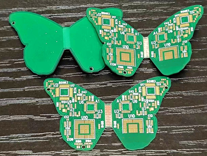
Curved PCB
What Are Curved PCBs?
Curved PCBs are printed circuit boards designed or formed to follow a curved, cylindrical, or otherwise non-flat geometry. Unlike conventional rigid PCBs, which are generally manufactured as flat panels, curved designs allow electronic circuits to conform to the shape of a product or enclosure. Depending on the application, the curvature may be built into a rigid board during a specialized manufacturing process, achieved through a flexible or rigid-flex PCB structure, or created by assembling multiple boards along a curved surface.
It is important to distinguish between a curved rigid PCB and a flexible PCB. A curved rigid board maintains its intended three-dimensional shape and is not necessarily designed to bend repeatedly. A flexible PCB, by contrast, uses bendable materials such as polyimide to accommodate flexing or folding. Rigid-flex designs combine rigid component-supporting areas with flexible interconnections. Selecting the appropriate structure depends on whether the product requires a permanently curved shape, occasional installation bending, or repeated dynamic movement.
From an engineering perspective, curvature affects more than the physical outline of a board. It can influence component placement, copper stress, dielectric spacing, impedance control, heat dissipation, and the way the board is supported inside an enclosure. Therefore, curved PCB design should be considered a coordinated mechanical, electrical, and manufacturing task rather than a purely aesthetic modification.
Why Curved PCBs Matter in Modern Electronics
One of the main reasons manufacturers consider curved circuit boards is space optimization. In compact products, a flat PCB may leave unused gaps around cylindrical batteries, curved housings, or irregular internal structures. A board that follows the available geometry can improve packaging efficiency and potentially reduce the overall product size. This is particularly valuable in wearable electronics, smart devices, automotive interiors, and specialized industrial equipment.
Curved designs can also support more distinctive product appearances. For example, a curved electronic module may fit behind a contoured dashboard, follow the shape of a wearable device, or integrate into a compact lighting assembly. By aligning the circuit board with the product enclosure, engineers can sometimes reduce the number of separate brackets, connectors, or mounting structures required.
However, curvature should not be adopted simply because it looks innovative. A well-designed flat PCB may still offer lower manufacturing costs, simpler inspection, and better component accessibility. Curved construction is most beneficial when the three-dimensional geometry solves a genuine packaging, integration, or functional problem that a conventional board cannot address efficiently.
Key Performance Benefits of Curved PCBs
The primary advantage of a curved circuit board is its ability to combine electronic functionality with three-dimensional product geometry. By following the contours of a housing, it can help engineers use internal space more efficiently, simplify certain assembly arrangements, and create compact electronic products. In applications where every millimeter matters, this flexibility can be more valuable than the board’s physical appearance alone.
Electrical performance can also benefit when the design reduces unnecessary connectors and cable interconnections. Fewer interconnects may reduce potential contact failures and signal discontinuities, particularly in compact or vibration-prone assemblies. Nevertheless, curvature itself does not automatically improve signal integrity. High-speed signals still require controlled impedance, suitable dielectric materials, continuous return paths, and careful routing.
Thermal performance requires similar attention. A curved board may fit closer to a metal enclosure or heat-spreading surface, potentially improving heat transfer when the mechanical interface is properly designed. Conversely, restricted airflow or reduced contact with a heat sink can create localized hot spots. Thermal simulations and testing under actual operating conditions are therefore important for power electronics, LED lighting, and automotive applications.
Mechanical reliability is another consideration. A properly designed curved structure can distribute components within a compact enclosure and reduce the need for additional mounting hardware. However, excessive bending stress, unsuitable materials, and poorly supported components can cause copper cracking, solder-joint fatigue, or delamination. The real performance benefit comes from matching the board structure to its operating environment, not from curvature alone.
Curved PCBs Manufacturing Costs and Key Factors
The cost of manufacturing a curved circuit board depends on its construction, material selection, geometry, production volume, and inspection requirements. A simple curved rigid board produced using a suitable forming process may have a very different cost structure from a multilayer rigid-flex assembly with complex three-dimensional geometry. Therefore, manufacturers should evaluate the complete design rather than estimate cost based only on board dimensions.
Material selection is a major cost factor. Standard FR-4 is widely used for conventional rigid boards, but it cannot be assumed suitable for every forming process. Flexible sections commonly require polyimide-based materials, while high-frequency applications may require specialized low-loss laminates. Higher-performance materials can increase raw material costs and require tighter process controls.
Layer count and circuit complexity also influence pricing. More copper layers, fine-pitch features, controlled-impedance routing, and complex interconnections increase fabrication and inspection demands. If the design requires rigid-flex construction, additional lamination steps, coverlay processing, specialized tooling, and tighter registration tolerances may add costs.
Forming and assembly requirements can create further expenses. Complex radii, tight dimensional tolerances, custom fixtures, and restricted component-placement areas may increase setup time and reduce manufacturing yield. Components placed close to a bend or curved transition can also complicate assembly and inspection.
Finally, production volume and quality requirements affect the unit price. Prototypes often have higher per-unit costs because engineering reviews, tooling, and process qualification are distributed across fewer boards. For mass production, standardized geometry, early design-for-manufacturability (DFM) reviews, and repeatable forming processes can improve consistency and reduce waste.
The most effective cost strategy is to define the required curvature early, select materials that support the intended geometry, and confirm the manufacturing method with the PCB supplier before finalizing the layout.
Curved PCBs Production Challenges and Practical Solutions
Although curved boards offer design flexibility, their manufacturing process introduces challenges that conventional flat PCBs may not encounter. Addressing these risks during engineering review is essential for preventing defects, unnecessary rework, and field failures.
Copper cracking and excessive mechanical strain are common concerns when a flexible circuit is bent too tightly or repeatedly. Copper traces experience tensile and compressive stresses during bending, and the risk increases when the bend radius is too small or the circuit structure is too thick. The solution is to specify the intended bend radius, distinguish between static and dynamic bending, select appropriate copper and dielectric materials, and keep vias and other stress-sensitive features away from active bend zones where possible. The correct design limits must be established for the specific stackup rather than applying one universal radius.
Delamination and dimensional distortion can occur when materials, bonding systems, or forming conditions are unsuitable. Uneven pressure, excessive process temperatures, and incompatible material combinations may affect layer adhesion or cause the finished board to deviate from its intended shape. Manufacturers should validate the material stackup, control lamination and forming parameters, and inspect the board against the specified three-dimensional geometry.
Solder-joint and component damage may arise if mechanical stress reaches populated areas during installation or operation. Components should generally be kept away from regions expected to experience significant bending, and the board should be supported appropriately within the enclosure. Where the design requires a flexible interconnection, rigid-flex construction can help isolate component-bearing regions from the bend zone.
Electrical variation and signal-integrity problems may occur when curvature changes the physical relationship between conductors, dielectric materials, and ground structures. This is especially important for high-speed digital signals and RF circuits. Engineers should evaluate the final geometry, maintain controlled impedance where required, preserve return paths, and validate critical designs using appropriate simulation and measurement.
Low production yield and assembly difficulties can result from incomplete design information. A two-dimensional fabrication drawing may not fully communicate the required shape, forming direction, installation constraints, or allowable tolerances. Providing three-dimensional CAD data, detailed mechanical drawings, bend specifications, and prototype samples helps the manufacturer identify potential conflicts before production begins.
Ultimately, the most reliable approach is collaborative engineering. PCB designers, mechanical engineers, assembly teams, and fabrication suppliers should review the same requirements before tooling and production are approved.
Curved PCBs Applications Across Different Industries
Wearable Electronics
Smartwatches, fitness trackers, and compact health-monitoring devices often use curved housings to fit comfortably against the body. Curved or flexible circuit structures can help accommodate these shapes while reducing unused internal space. Designers must still consider moisture protection, battery placement, heat generation, and long-term mechanical durability.
Automotive Electronics
Curved circuit structures can be useful in dashboard displays, ambient lighting, sensor modules, and compact electronic control assemblies. Their ability to fit irregular spaces can support more integrated vehicle interiors. Automotive applications require particular attention to vibration, thermal cycling, humidity, and long-term reliability.
LED Lighting and Industrial Equipment
Curved boards can support circular lighting fixtures, cylindrical products, and specialized industrial instruments. In these applications, board geometry must be coordinated with heat dissipation, mounting strength, and electrical insulation to maintain consistent performance.
Medical and Aerospace Electronics
Compact medical instruments and aerospace systems may require electronic assemblies that follow complex internal contours. Flexible or rigid-flex solutions can simplify routing through confined spaces, but material qualification, inspection, environmental resistance, and application-specific reliability requirements remain essential.
These applications illustrate an important principle: the right curved design is determined by the product’s mechanical constraints, electrical requirements, and operating environment. A curved rigid board may suit a permanently shaped module, while a flexible or rigid-flex design may be more appropriate when bending or folding is part of the assembly process.
Curved PCBs Design and Supplier Selection Considerations
Selecting an experienced PCB manufacturing partner can reduce the risk of design errors and production delays. A capable supplier should be able to review the board’s intended three-dimensional shape, recommend suitable materials, evaluate layer construction, and identify features that may create manufacturing difficulties.
Before placing an order, provide the supplier with the Gerber files, stackup information, mechanical drawings, three-dimensional CAD data where applicable, and the required dimensional tolerances. Clarify whether the board will be permanently formed, bent once during installation, or repeatedly flexed during operation. These distinctions influence material selection, forming methods, testing, and expected service life.
For demanding designs, prototype validation is especially valuable. A prototype can reveal interference with the enclosure, component-clearance problems, unexpected stress concentrations, and difficulties during assembly. Electrical testing should be combined with mechanical and thermal evaluation where the application requires it.
SQ PCB can be considered as a manufacturing partner for customized PCB requirements, including rigid and multilayer board designs. When evaluating any supplier for a curved application, confirm its experience with the specific board construction and forming process required, rather than relying on general PCB production capabilities alone.
Conclusion
Curved circuit boards offer an effective way to address the growing demand for compact, integrated, and visually distinctive electronic products. By following a product’s three-dimensional geometry, they can improve space utilization, simplify certain interconnection arrangements, and support innovative designs across wearable electronics, automotive systems, lighting, medical devices, and industrial equipment.
However, successful implementation requires careful engineering. Material compatibility, bend radius, copper routing, layer structure, thermal management, dimensional tolerances, and manufacturing yield all influence the final result. A board that fits the enclosure perfectly but develops cracked traces, unstable electrical characteristics, or poor heat dissipation will not deliver lasting value.
The best strategy is to begin with the product’s functional requirements, choose between curved rigid, flexible, and rigid-flex construction, and involve the manufacturer before the design is finalized. Early DFM review, prototype testing, and clearly defined acceptance criteria can help reduce avoidable costs and improve product reliability.
For businesses developing next-generation electronics, curved PCB technology is not simply a design trend. It is a practical engineering option when three-dimensional integration solves a real product challenge. With the right structure, manufacturing process, and quality controls, the benefits of curved circuit design can extend beyond appearance to packaging efficiency, assembly simplicity, and dependable long-term performance.
FAQs
1. What are Curved PCBs used for?
They are used in electronic products that require circuit boards to follow curved or irregular surfaces. Common applications include wearable devices, automotive lighting, dashboard electronics, medical instruments, industrial equipment, and specialized compact assemblies.
2. Are Curved PCBs the same as flexible PCBs?
No. A curved rigid PCB maintains a fixed shape and may be manufactured using a specialized forming process. A flexible PCB uses bendable materials, typically polyimide, and may accommodate bending during installation or operation. Rigid-flex PCBs combine rigid component-supporting areas with flexible interconnections.
3. What factors affect the cost of Curved PCBs?
The main factors include substrate and copper materials, layer count, circuit complexity, forming method, curvature and dimensional tolerances, tooling, inspection requirements, production volume, and expected yield. Complex rigid-flex constructions generally require more specialized processing than conventional rigid boards.
4. What manufacturing problems can occur with Curved PCBs?
Potential problems include copper cracking, delamination, dimensional distortion, component or solder-joint damage, signal-integrity variation, and low manufacturing yield. These risks can be reduced through suitable material selection, correct bend-radius design, careful copper routing, process validation, and prototype testing.
5. How can engineers improve Curved PCBs reliability?
Engineers should define the final three-dimensional geometry early, confirm the intended forming or bending conditions, select compatible materials, and avoid placing stress-sensitive features in high-strain regions. They should also review thermal management and signal integrity, collaborate with the manufacturer during DFM review, and validate prototypes under representative operating conditions.

- Special PCB
- long board pcb
- Flexible PCBs
- Special PCB
- Express Printed Circuit Board
- Pcb Prototype
- LED PCB
- PCB
- Pcb Meaning
- Printed Circuit Board
- Pcb manufacturer
- Rigid pcb board
 Quote
 E-mail