Introduction
As PCB designs become smaller, denser, and more electrically demanding, manufacturing precision has become just as important as circuit design. This is especially true for HDI PCBs, where fine traces, narrow spacing, microvias, and high routing density leave very little room for process variation.
Among the many steps in PCB fabrication, etching may appear straightforward: remove unwanted copper and keep the copper protected by the circuit pattern. In reality, the etching profile directly affects trace width, spacing, impedance, yield, and long-term reliability. Alkaline copper etching, typically based on ammonia/ammonium chloride and copper chloride chemistry, is widely used where controlled copper removal and compatibility with metallic resist systems are required.
For manufacturers and PCB buyers, understanding this process is therefore not simply a chemistry question. It is a question of how accurately a production line can convert a digital PCB design into a physical circuit.
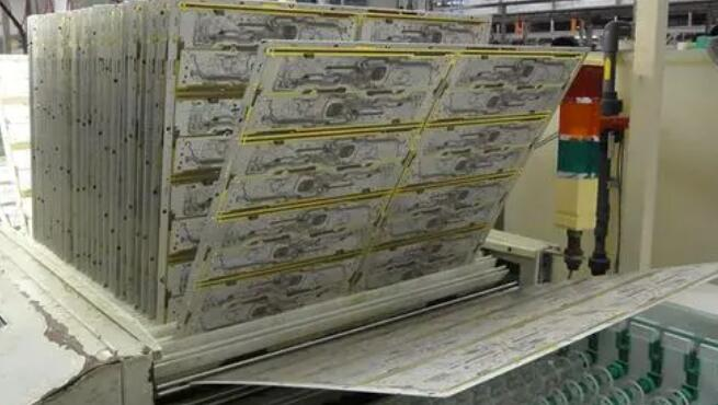
PCB Alkaline Etching
What Is Alkaline Etching and How Does It Work?
Alkaline Etching is a controlled chemical process used to remove unwanted copper from a PCB while preserving the copper areas protected by an etch-resistant pattern. A typical ammoniacal system uses copper chloride together with ammonia and ammonium chloride. Ammonia forms copper-ammine complexes that keep copper in solution and support continuous etching and regeneration.
In a typical outer-layer fabrication flow, the PCB first undergoes imaging and pattern plating. After the unwanted resist is removed, exposed copper is selectively dissolved in the etching chamber. The remaining copper becomes the required conductive pattern.
The important point is that etching is not perfectly vertical. Copper can be removed laterally underneath the protected pattern, creating undercut. As line widths become smaller, even a relatively small amount of lateral copper loss can significantly change the final conductor geometry. Process parameters such as pH, copper concentration, chloride concentration, temperature, spray pressure, conveyor speed, and nozzle condition therefore need to be controlled together.
In my view, this is why etching deserves more attention than it usually receives. Designers may spend considerable effort optimizing stackups, materials, impedance, and routing, but the final physical trace still depends on how accurately the manufacturing process reproduces the artwork.
Why Alkaline Etching Matters for HDI PCB Fabrication
HDI manufacturing is particularly sensitive to etching variation because the available design margin becomes increasingly small. Fine lines and spaces mean that a few microns of unwanted copper removal can have a much larger relative effect than it would on a conventional PCB.
A well-controlled alkaline process can help manufacturers maintain more consistent conductor geometry and reduce the risk of excessive undercut. This is important for applications involving fine-pitch components, high-I/O devices, compact modules, and impedance-controlled high-speed circuits.
The relationship can be summarized simply:
| Manufacturing factor | Potential impact on HDI PCB |
|---|---|
| Excessive undercut | Trace width reduction and possible opens |
| Uneven etching | Panel-to-panel or area-to-area variation |
| Over-etching | Reduced conductor cross-section |
| Under-etching | Copper residues and possible shorts |
| Poor spray uniformity | Uneven line definition |
| Unstable chemistry | Changing etch rate and dimensional variation |
| Inadequate process monitoring | Lower production consistency |
For high-density boards, precision is not only about achieving a minimum line/space specification once. The real challenge is repeating that specification consistently across the entire panel and production batch.
Alkaline Etching Cost Factors and PCB Performance Impact
The cost of the process should not be evaluated only by the price of the etching chemicals. A realistic manufacturing cost includes chemical consumption, equipment, ventilation, process monitoring, replenishment, wastewater treatment, maintenance, production speed, yield, and inspection.
Ammoniacal systems can offer high copper-loading capability and compatibility with certain metallic resists, but ammonia management and waste treatment add operational considerations. Exhaust handling is also important because ammonia-containing systems require appropriate ventilation and control.
At the same time, spending slightly more on process control can sometimes reduce the much larger cost associated with rejected panels or electrical failures.
| Cost factor | What manufacturers should consider |
|---|---|
| Chemicals | Etchant consumption and replenishment rate |
| Equipment | Spray system, pumps, filters, controls, and ventilation |
| Process control | pH, copper concentration, temperature, and etch rate |
| Waste treatment | Copper- and ammonia-containing wastewater |
| Yield | Scrap caused by shorts, opens, or dimensional variation |
| Inspection | Cross-section analysis and line-width measurement |
| Production speed | Etch rate and conveyor throughput |
| Maintenance | Nozzle, pump, filter, and chamber condition |
From a PCB buyer’s perspective, the most meaningful number is often cost per qualified board, rather than the cost of the etching chemistry itself.
The electrical impact is equally important. If a conductor becomes narrower than intended, its resistance and current-carrying capability can change. In controlled-impedance applications, changes in conductor geometry can also affect impedance and signal behavior. Excessive etching may therefore create problems that are not immediately visible during visual inspection.
Common Alkaline Etching Problems and Practical Solutions
The biggest challenge is maintaining a stable relationship between chemistry and equipment. A bath that performs well at the beginning of a production run may behave differently as copper loading, temperature, pH, and chemical balance change.
1. Excessive undercut
Excessive lateral etching can reduce finished trace width and compromise fine-line structures. The solution is to monitor the etch rate and chemical parameters continuously while optimizing spray pressure, temperature, conveyor speed, and chemistry concentration.
2. Incomplete copper removal
If the etching process is too weak or the exposure time is insufficient, residual copper may remain between adjacent features. This can increase the risk of electrical shorts. Regular etch-rate verification and proper equipment calibration are essential.
3. Uneven etching across the panel
Nozzle blockage, uneven spray pressure, poor panel loading, or chamber contamination can create different etching conditions in different areas. Preventive maintenance and spray-pattern inspection can significantly reduce this risk.
4. Chemistry instability
Changes in pH, copper concentration, chloride concentration, or temperature can change the etching behavior. Automated monitoring and controlled replenishment are preferable to relying only on manual adjustment. Technical literature and process guidance specifically identify these variables as important factors affecting etch rate and undercut.
5. Copper sludge and equipment contamination
Poor chemical balance can contribute to deposits that interfere with pumps, filters, or spray nozzles. Regular filtration, bath management, and preventive cleaning help maintain stable production.
In my opinion, the most effective strategy is not to wait for a finished PCB to reveal an etching problem. Process capability should be controlled before defects become visible. Monitoring line width, etch rate, chemical conditions, and equipment performance gives manufacturers a much better opportunity to prevent defects instead of simply sorting them afterward.
How Alkaline Etching Supports Better HDI Manufacturing
For HDI production, successful etching should be viewed as part of an integrated manufacturing chain rather than an isolated chemical operation.
Imaging accuracy, resist quality, copper thickness, etching conditions, inspection, and final electrical testing all interact. A highly accurate exposure process cannot compensate for uncontrolled etching, just as excellent etching cannot correct an improperly designed artwork.
A practical HDI manufacturing strategy should therefore include:
- Design rules that match the manufacturer’s actual process capability.
- Controlled copper thickness before etching.
- Stable resist imaging and development.
- Continuous monitoring of etching chemistry.
- Regular spray-nozzle and conveyor maintenance.
- Line-width and spacing verification.
- Cross-section analysis for critical designs.
- Electrical testing after fabrication.
- Statistical monitoring for production consistency.
This process-oriented approach is especially valuable when customers require repeat orders. The objective should not simply be to make one good prototype, but to establish a manufacturing window that can reliably reproduce the same geometry at production volume.
When Alkaline Etching Becomes Especially Important
The value of this process becomes more apparent as PCB geometry becomes more demanding. Fine-line HDI boards, compact consumer electronics, advanced modules, and impedance-sensitive circuits can all place greater demands on conductor definition.
However, it is important not to treat one etching chemistry as universally superior. Different PCB structures, copper thicknesses, resist systems, line/space requirements, production volumes, and environmental controls can lead manufacturers toward different process choices. Industry references also describe different etching systems being selected according to layer structure, resist compatibility, fine-line requirements, waste management, and production considerations.
The better question is therefore not simply “Which etchant is best?” but rather “Which etching process provides the required geometry, yield, reliability, and total manufacturing cost for this particular PCB?”
Conclusion
The importance of Alkaline Etching in HDI PCB fabrication goes far beyond removing unwanted copper. It is one of the manufacturing steps that determines whether a highly optimized PCB design can actually be reproduced accurately on a production panel.
As line widths and spaces continue to shrink, the manufacturing margin becomes smaller. Excessive undercut can reduce conductor width, unstable chemistry can create dimensional variation, and inadequate equipment maintenance can turn a theoretically capable process into an inconsistent one. These problems can eventually appear as opens, shorts, impedance variation, reduced current capacity, lower yield, or reliability concerns.
For PCB manufacturers, the answer is not simply to use more aggressive chemistry. It is to establish a controlled process window through chemical monitoring, equipment maintenance, accurate imaging, dimensional inspection, and continuous process improvement.
For PCB buyers, this is also an important supplier-evaluation point. When comparing manufacturers, asking about fine-line capability alone is not enough. It is worth understanding how the manufacturer controls etching, verifies finished trace geometry, manages chemical stability, and maintains consistency from prototype to mass production.
That is the real reason this process deserves attention: HDI performance ultimately depends on manufacturing precision. When the chemistry, equipment, materials, and process controls work together, etching becomes not merely a subtractive step, but an important enabler of smaller, denser, and more reliable electronic products.
FAQs
1. What is Alkaline Etching in PCB manufacturing?
It is a chemical copper-removal process that uses an alkaline ammoniacal system, commonly involving copper chloride, ammonia, and ammonium chloride. It removes exposed copper while protecting the desired circuit pattern.
2. Why is Alkaline Etching important for HDI PCBs?
HDI boards use fine traces and narrow spaces, so small variations in copper removal can significantly affect finished conductor dimensions. Stable etching helps manufacturers maintain more consistent line width, spacing, and electrical characteristics.
3. What causes undercut during Alkaline Etching?
Undercut occurs because the etchant removes copper not only vertically but also laterally beneath the protected pattern. Chemistry, temperature, spray conditions, etch time, copper thickness, and equipment condition can all influence the final profile.
4. How can PCB manufacturers reduce Alkaline Etching defects?
Manufacturers can reduce defects by controlling pH, copper concentration, chloride concentration, temperature, spray pressure, conveyor speed, and chemical replenishment. Regular nozzle maintenance and line-width inspection are also important.
5. Does Alkaline Etching increase PCB manufacturing cost?
It can add costs related to chemicals, equipment, ventilation, process monitoring, and wastewater treatment. However, effective process control can reduce scrap and improve yield, so the total manufacturing cost should be evaluated based on the cost of producing qualified PCBs rather than chemistry cost alone.

- Special PCB
- long board pcb
- Flexible PCBs
- Special PCB
- Express Printed Circuit Board
- Pcb Prototype
- LED PCB
- PCB
- Pcb Meaning
- Printed Circuit Board
- Pcb manufacturer
- Rigid pcb board
 Quote
 E-mail